
Unveiling the Secrets of Atomic Layer Deposition for Semiconductor Fabrication

Atomic Layer Deposition (ALD) has emerged as a revolutionary technology in the semiconductor industry, enabling the fabrication of advanced materials and devices with unprecedented precision and control. This comprehensive guide provides an in-depth exploration of the principles, techniques, and applications of ALD in semiconductor manufacturing.
5 out of 5
| Language | : | English |
| File size | : | 9306 KB |
| Text-to-Speech | : | Enabled |
| Enhanced typesetting | : | Enabled |
| Print length | : | 479 pages |
| Screen Reader | : | Supported |
| Paperback | : | 492 pages |
| Item Weight | : | 1.92 pounds |
| Dimensions | : | 7.44 x 0.99 x 9.69 inches |
Fundamentals of ALD
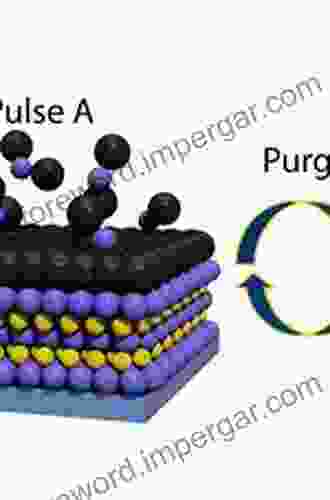
ALD is a chemical vapor deposition (CVD) technique that involves the sequential deposition of thin films by alternating pulses of precursor gases. The self-limiting nature of ALD ensures that each atomic layer is deposited in a highly conformal and uniform manner, resulting in precise control over film thickness and composition.
Key Principles
- Sequential Pulses: Precursor gases are introduced sequentially into the deposition chamber, allowing for the formation of alternating atomic layers.
- Self-Limiting Reactions: Surface reactions are self-limiting, resulting in the deposition of a single atomic layer per pulse.
- Atomic Layer Precision: Layer-by-layer deposition enables precise control over film thickness and composition.
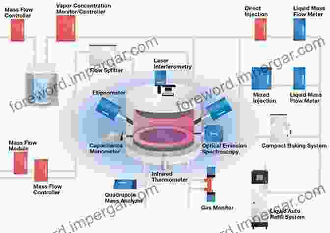
ALD Techniques
ALD can be performed using various techniques, each with its own advantages and applications. The most common techniques include:
Thermal ALD
Thermal ALD utilizes high temperatures to promote surface reactions and film growth. It offers high deposition rates and excellent film quality.
Plasma-Enhanced ALD
Plasma-enhanced ALD introduces a plasma into the deposition chamber to enhance surface reactions and enable low-temperature deposition. This technique is particularly suitable for materials with low thermal stability.
Remote Plasma ALD
Remote plasma ALD separates the plasma from the substrate, reducing damage to sensitive materials. This technique is ideal for depositing thin films on delicate substrates.
Photo-Assisted ALD
Photo-assisted ALD utilizes light energy to initiate surface reactions, enabling the deposition of materials at room temperature. This technique is promising for flexible electronics and other applications where low-temperature deposition is crucial.
Materials and Applications
ALD has found widespread applications in semiconductor manufacturing, particularly in the deposition of:
High-κ Dielectrics
ALD enables the deposition of high-κ dielectric materials, such as hafnium oxide and aluminum oxide, with superior electrical properties and reduced leakage currents.
Metal Gate Electrodes
ALD can deposit metal gate electrodes, such as titanium nitride and tungsten, with high work functions and excellent barrier properties.
Metal Interconnects
Copper and other metal interconnects can be deposited via ALD with improved conductivity, reduced resistance, and resistance to electromigration.
Semiconductor Nanostructures
ALD enables the fabrication of semiconductor nanostructures, such as quantum dots and nanowires, with precise control over size, shape, and composition.
Advantages and Benefits
ALD offers numerous advantages over other deposition techniques, including:
- Atomic Layer Precision: Enables precise control over film thickness and composition.
- Uniformity and Conformality: Provides highly conformal and uniform films, even on complex structures.
- Scalability: Applicable to large-scale manufacturing processes.
- Low-Temperature Deposition: Some techniques allow for deposition at low temperatures, reducing thermal stress and damage.
- Wide Material Compatibility: Can deposit a wide range of materials, including metals, oxides, nitrides, and sulfides.
Challenges and Limitations
While ALD offers significant advantages, it also faces certain challenges and limitations:
- Deposition Rates: ALD can be slower than other deposition techniques, especially for thick films.
- Precursor Availability: The availability of suitable precursors for specific materials can limit the implementation of ALD.
- Equipment Complexity: ALD equipment can be complex and require specialized expertise to operate.
Future Prospects
ALD research and development continue to advance rapidly, with promising advancements in:
- Novel Materials: Exploring new materials and precursors to expand the range of applications.
- Low-Temperature Deposition: Developing techniques for low-temperature deposition on flexible and other sensitive substrates.
- Scalable Manufacturing: Optimizing processes for high-volume manufacturing.
- Integration with Other Techniques: Combining ALD with other deposition techniques for enhanced performance and functionality.
Atomic Layer Deposition has revolutionized the semiconductor industry, enabling the fabrication of advanced materials and devices with unprecedented precision and control. This comprehensive guide has provided an in-depth exploration of the principles, techniques, and applications of ALD in semiconductor manufacturing, highlighting its advantages, challenges, and future prospects.
With ongoing advancements and research, ALD is poised to play an even more significant role in the development of next-generation electronic devices and technologies.
5 out of 5
| Language | : | English |
| File size | : | 9306 KB |
| Text-to-Speech | : | Enabled |
| Enhanced typesetting | : | Enabled |
| Print length | : | 479 pages |
| Screen Reader | : | Supported |
| Paperback | : | 492 pages |
| Item Weight | : | 1.92 pounds |
| Dimensions | : | 7.44 x 0.99 x 9.69 inches |
Do you want to contribute by writing guest posts on this blog?
Please contact us and send us a resume of previous articles that you have written.
 Book
Book Novel
Novel Page
Page Chapter
 Text
Text Story
Story Genre
Genre Reader
 Library
 Paperback
 E-book
 Magazine
 Newspaper
 Paragraph
 Sentence
 Bookmark
 Shelf
Shelf Glossary
 Bibliography
 Foreword
 Preface
 Synopsis
 Annotation
 Footnote
 Manuscript
 Scroll
 Codex
Codex Tome
Tome Bestseller
 Classics
 Library card
 Narrative
 Biography
 Autobiography
 Memoir
 Reference
 Encyclopedia
 Mike Madison
 Eileen Welsome
 Edward Samuel Corwin
 Lynn Louise Wonders
 Jean Barbre
 Jean Blacklock
 Michael Grecco
 Eric H Cline
 Lawrence Wallace
 Geri Walton
 Gary J Byrne
 Elizabeth Thomson
 Elissa Stacy
 Elaine Storkey
 Erin Entrada Kelly
 Mary E Guy
 George Charalambous
 Enrico Dal Lago
 Sue J Daniels
 Joann K Whalen
Light bulbAdvertise smarter! Our strategic ad space ensures maximum exposure. Reserve your spot today!


 Miguel NelsonMothers of Massive Resistance: The True Story of the White Women Who Led the...


 Branden SimmonsFollow ·4.3k
 Donald WardFollow ·19k
 Frank ButlerFollow ·17.2k
 Blake BellFollow ·19.5k
 Jean BlairFollow ·18.4k
 Samuel WardFollow ·11.6k
 Ron BlairFollow ·3.5k
 Fernando BellFollow ·3.8k

 Bob Cooper
Unlock the Secrets to Nurturing Highly Successful...
In a rapidly evolving world where...

 Mario Simmons
The Fall of the Hellenistic Kingdoms 250-31 BC: A...
Unraveling...

 Glen Powell
Unveiling the Profound Connection: Health and Emotions
In today's fast-paced...

 Gavin Mitchell
Step Back in Time: Experience the Vietnam War Through...
Uncover the Raw...
 Robert Frost
The Forgotten 1989 Expulsion Of Turks From Communist...
Unveiling a Hidden Chapter...
 Deacon Bell
24 Hours in Ancient Athens
A Day in the Life of a Classic Civilization ...
5 out of 5
| Language | : | English |
| File size | : | 9306 KB |
| Text-to-Speech | : | Enabled |
| Enhanced typesetting | : | Enabled |
| Print length | : | 479 pages |
| Screen Reader | : | Supported |
| Paperback | : | 492 pages |
| Item Weight | : | 1.92 pounds |
| Dimensions | : | 7.44 x 0.99 x 9.69 inches |
